Lumilens came out of stealth on August 6 with more than 900 million dollars raised, a 5.51 billion dollar valuation, and something rarer than either: product already shipping into a hyperscaler's production data centres under a multi billion dollar agreement. The company was founded in early 2024, which makes that timeline unusual for silicon photonics. The pitch from founder Ankur Singla is a single sentence worth arguing with, that the constraint on AI has shifted from how many GPUs you can buy to how many you can connect. We looked at what the company actually builds, and where optics sit in an AI cluster.
The short answer
Lumilens left stealth on August 6 with more than 900 million dollars raised and a 5.51 billion dollar valuation. Founded in early 2024 by Ankur Singla, it builds optical interconnect for both networks inside an AI data centre: near package and co-packaged optics for the scale up network that links accelerators, and 800G and 1.6T pluggable transceivers for the scale out fabric between racks. Its LumiCore platform covers silicon photonics, mixed signal ICs, electrical optical interposers and optical systems in house. Product is already shipping to a hyperscaler under a multi billion dollar agreement. No power or latency figures have been published.
Funding announcements from photonics startups usually read the same way, and the number is rarely the interesting part. What caught our attention in this one is a single clause buried under the valuation: the product is already in a hyperscaler's production data centres. Hyperscalers qualify optics with a thoroughness that borders on hostility, and a company founded in early 2024 does not usually clear that in two years.
Two networks, not one
An AI data centre runs two distinct networks and they have almost nothing in common except the building.
The scale up network connects accelerators to each other inside a single compute system. Its job is to make a rack of GPUs behave like one very large device, because the model does not fit on any single chip and every layer needs to exchange data with every other. Distances are short, bandwidth is enormous, and the metrics that decide the design are latency and picojoules per bit.
The scale out fabric connects those systems to each other across the hall. Longer reach, more familiar shape, closer to the Ethernet networking most engineers already know. Different optics, different packaging, different failure model.
Lumilens builds for both, which is the unusual choice. Near package optics and co-packaged optics on the scale up side, pluggable transceivers at 800G, 1.6T and beyond on the scale out side. Companies normally pick one, because the engineering problems only look related from a distance.
Why the optics keep moving closer to the chip
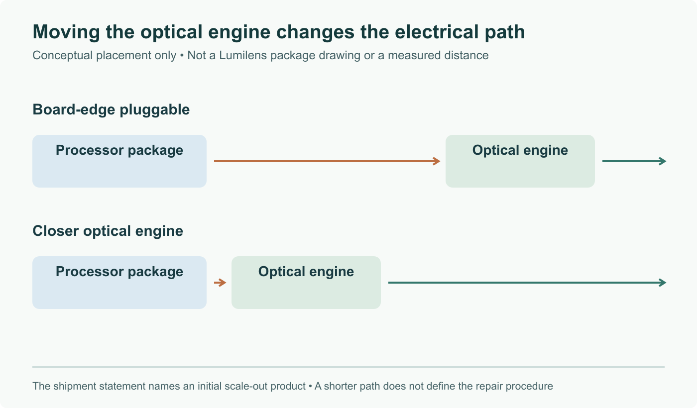
In a conventional design, switch or accelerator silicon drives an electrical signal across the board to a pluggable module at the faceplate. That copper run is a few centimetres, which was unremarkable at 100G and is a serious problem at 1.6T. Driving a clean signal that far costs power, and the cost grows faster than the line rate does.
Near package optics puts the optical engine on the same substrate as the chip. Co-packaged optics puts it in the same package. Either way the copper shrinks from centimetres to millimetres, and the power arithmetic starts working again.
The cost is serviceability, and it is a real cost rather than a rhetorical one. A pluggable transceiver that fails is a five minute swap by a technician who does not need to know what the machine does. A co-packaged optical engine that fails is bonded to a switch ASIC or an accelerator worth a great deal more, and the repair is a different conversation entirely. That trade is why the industry has spent years discussing co-packaged optics rather than deploying it, and it is why the deployment claim in this announcement matters more than the valuation.
The vertical bet
LumiCore, the company's platform, spans four things that are usually four suppliers: silicon photonics, mixed signal integrated circuits, electrical optical interposers, and the optical systems and manufacturing processes wrapped around them.
Building all of it is a demanding way to start. The argument for doing so is co design. When the driver circuit, the photonic device and the package are developed by the same team, requirements can be traded across the boundaries rather than accepted as fixed at each interface, and the interfaces are precisely where power and yield tend to leak. Lumilens says the result is a path from design to customer qualification measured in months rather than years, which if true is the more interesting claim in the announcement.
What to take from it
The framing from founder Ankur Singla is quotable and slightly too clean: the constraint on AI has shifted from how many GPUs you can buy to how many you can connect. Directionally that is right. Collective operations mean the slowest link paces the whole job, and an accelerator waiting on the network is capital sitting idle. As chips have got faster, the share of time spent moving data rather than computing has grown, which is how co-packaged optics went from a research track to a procurement line in about two years.
Where it oversells is in implying compute stopped mattering. It did not, and neither did memory bandwidth. A modern cluster has three ceilings, and interconnect is simply the one that tightened fastest.
For anyone who designs or operates this kind of infrastructure, the practical question is not whether optics move closer to the silicon, because they will. It is what your operational model looks like when a link failure stops being a module swap. That is the question to bring to any vendor conversation about co-packaged optics this year, and it is the one no funding round answers.
Sources and further reading
- Lumilens Emerges from Stealth with More Than 900 Million Dollars in Funding, Business Wire, August 6, 2026
- Lumilens emerges with 900M dollars in funding, company newsroom
- Lumilens Emerges from Stealth with 700M Raise, Targets Optical Interconnects, Converge Digest
- Lumilens debuts with 700M war chest and 5.5B valuation after emerging from stealth, Tech Funding News
- AI's bottleneck moved from chips to wiring, TNW
Frequently asked questions
What is the difference between scale up and scale out, and why does it matter here?
They are two different networks inside the same building, with different physics and different economics. The scale up network connects accelerators to each other inside a single compute system, a rack or a small group of racks, and it is what makes a set of GPUs behave like one large device for a model that does not fit on any single chip. It runs at very high bandwidth over very short distances, and latency and power per bit dominate everything else. The scale out fabric connects those systems to each other across the data hall, over longer reach, and looks much more like the Ethernet networking most people know. Lumilens builds for both, which is the notable part: near package and co-packaged optics for scale up, pluggable transceivers at 800G and 1.6T and beyond for scale out. Most optics companies pick one side, because the packaging problems barely resemble each other.
What are co-packaged and near package optics, in practical terms?
They are attempts to shorten the electrical path between the switch or accelerator silicon and the point where the signal becomes light. In a conventional design, the chip drives an electrical signal across the circuit board to a pluggable module at the faceplate, and that centimetres long copper run is where a growing share of the power budget and the signal integrity headaches live as line rates climb. Near package optics moves the optical engine onto the same substrate, close to the chip. Co-packaged optics moves it into the same package. Both shorten copper to something measured in millimetres, which is what makes the power arithmetic work at 1.6T and above. The trade is serviceability. A pluggable module that fails gets swapped in minutes by a technician, while a co-packaged engine that fails is attached to something far more expensive, which is exactly why the industry has been cautious and why shipping into a hyperscaler in production is the part of this announcement that carries real information.
How much should the funding number itself tell me?
Less than the customer agreement does. More than 700 million dollars in a Series C at a 5.51 billion dollar valuation, taking total funding above 900 million, is a large round in a market where large rounds are currently routine, and it was co led by Atreides Management, Bain Capital Ventures, Meritech, Seligman Ventures and Spark Capital, with Qualcomm Ventures, J.P. Morgan Private Capital, Mayfield, Peak XV, Redpoint and others joining. Investors funding an ambitious plan is not evidence the plan works. The line that carries weight is that Lumilens says it is already shipping product into a hyperscaler's production data centres under a multi billion dollar agreement, because hyperscalers qualify optics slowly and unforgivingly, and a company founded in early 2024 clearing that bar in roughly two years is either very good or very lucky with timing. Both are worth watching.
What is the LumiCore platform actually made of?
Four layers that most companies buy from four different suppliers. Silicon photonics, the waveguides and modulators that carry and shape light on a chip. Mixed signal integrated circuits, the drivers and receivers that sit between the digital world and the analogue optical one, which is where a great deal of the power consumption and most of the difficulty lives. Electrical optical interposers, the substrate that lets the electrical and optical dies sit together and talk. And the optical systems and manufacturing processes around all of it. Owning the whole stack is a heavy way to start a company, and the argument for it is co design: when the driver circuit, the photonic device and the package are developed together, you can trade requirements between them instead of accepting whatever interface each vendor happens to offer. Lumilens says this compresses the path from design to customer qualification into months rather than years.
Is the claim that networking, not compute, is the real AI bottleneck actually true?
It is directionally right and worth stating carefully. Training a large model splits work across thousands of accelerators, and every step involves collective operations where all of them exchange gradients or activations before anyone proceeds. That pattern means the slowest link sets the pace for the entire job, and it means an accelerator waiting on the network is an accelerator you paid for and are not using. As individual chips have got faster, the fraction of time spent moving data rather than computing has grown, which is why co-packaged optics went from research topic to procurement conversation in a couple of years. Where the framing oversells is in suggesting compute has stopped mattering. It has not, and neither has memory bandwidth. The honest version is that a cluster has three ceilings now instead of one, and interconnect is the one that got tighter fastest. Lumilens has published no public power per bit or latency figures, so treat the technical claims as unquantified until the numbers arrive.