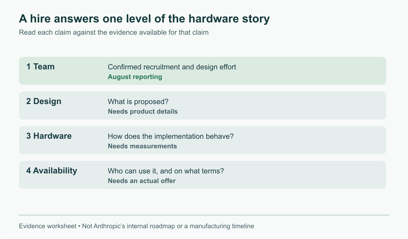
Anthropic has hired Amir Salek, the engineer Google recruited in 2013 to start its custom silicon effort and who went on to deliver the first seven generations of the Tensor Processing Unit. Bloomberg reported the move on Friday, August 21, 2026, and it was widely carried the following day. Salek joins Anthropic's compute team and reports to James Bradbury. The timing is the part worth reading closely: the hire lands about two weeks after Anthropic publicly confirmed it was assembling an in-house chip design team and started advertising silicon roles at up to 485,000 dollars a year, asking specifically for engineers who have shipped real hardware.
The short answer
Bloomberg reported on Friday, August 21, 2026 that Anthropic hired Amir Salek, who started Google's custom silicon effort in 2013 and is credited with delivering the first seven generations of the Tensor Processing Unit before leaving that business in 2022. He joins Anthropic's compute team and reports to James Bradbury. The hire follows by about two weeks the public confirmation that Anthropic is assembling an in-house chip design team, with silicon roles advertised at reported salaries between 320,000 and 485,000 dollars.
Job listings tell you what a company wants. The person it hires tells you how serious it was.
The hire, and what the record says about him
Salek is not a general purpose executive brought in for a hardware initiative. Google recruited him in 2013 specifically to start its custom silicon programme from the ground up, and reporting credits him with the first seven generations of the Tensor Processing Unit before he left that business in 2022. Before Google he spent roughly eight years at Nvidia, where he founded and led a system on a chip design group covering graphics and Tegra parts. After Google he moved to Cerberus Capital Management as a senior managing director, investing in semiconductor, AI and aerospace companies.
At Anthropic he joins the compute team, reporting to James Bradbury. No title or roadmap has been published, so it is worth resisting the temptation to infer a product from a personnel move. What can be said is narrower and still meaningful: a company that has decided to design silicon just hired someone with direct experience of doing it from nothing, twice, at companies whose scale it now approaches.
The other detail in his history that matters is the seven generations. Starting a chip programme is a well documented skill. Sustaining one across seven generations, with all the compatibility and toolchain debt that accumulates, is a different and rarer one, and it is the harder half of what Anthropic would need.
The two weeks before
The sequence is what makes this readable. In early August 2026 Anthropic publicly confirmed that it was putting together an in-house chip design team, and the job listings were unusually specific about what it wanted. They asked for silicon engineers and hardware system architects who had personally contributed to finalising and shipping a semiconductor design, at salaries reported between 320,000 and 485,000 dollars a year. One listing described the role as suited to someone who has shipped silicon, has a realistic relationship with schedules, and is comfortable making consequential calls without a large organisation behind them.
That last clause reads differently now. It describes a small team expected to make decisions at speed, which is exactly the environment somebody who started a chip programme inside a large company might prefer the second time around.
The stated goal is co-design: hardware shaped around how Claude actually runs, so that inference gets faster and cheaper than it would on a general purpose part. That is the same argument Google made for the TPU, which is not a coincidence given who is now in the building.
What it means for the compute market
Anthropic runs an unusually broad mix of hardware today. Coverage of the chip team notes Nvidia and AMD GPUs, Google TPUs and Amazon Trainium in production use. Four accelerator families is a lot of porting work to carry, and companies do not carry it by accident.
It also produces something valuable: comparative data. A team that has run the same workloads across four architectures knows in detail where each one wastes silicon on its particular inference stack. That is a much better starting position for a custom design than a team extrapolating from one vendor, and it is probably the strongest practical argument that this effort is more than a hedge.
For everyone else, the trend line is the useful part. The companies building the largest models are steadily moving down the stack, first into data centre construction, then into power, now into the accelerators themselves. Each step is a bet that the layer below is not being optimised for them fast enough. Whether that is true says more about the pace of the general purpose roadmap than about any single hire.
What we would take from this
Treat a chip team as a schedule, not an announcement. Silicon takes years from a staffed team to a part running production traffic, and the gap between confirming a team in August 2026 and running your own accelerator is long enough for the model architecture it was designed around to change.
The counterweight is the reason to do it anyway. If inference cost is the dominant line in your economics, and it increasingly is, then a percentage improvement in efficiency compounds across every request forever. That is the kind of maths that justifies hiring the person who has already done it seven times.
Sources and further reading
- Anthropic Taps Google Chip Veteran as Part of Push Into Hardware, Bloomberg, August 21, 2026
- Anthropic taps Google chip veteran Amir Salek as part of push into hardware, Business Standard, August 22, 2026
- Anthropic Eyes Its Own AI Chips: Why It Hired a Google Chip Veteran, Outlook Business
- Anthropic publicly confirms it is putting together an in-house chip design team, Data Center Dynamics
- Anthropic is hiring an AI chip design team, TechCrunch, August 5, 2026
Frequently asked questions
Who is Amir Salek?
He is the engineer Google brought in during 2013 to build its custom silicon effort from nothing, and reporting credits him with delivering the first seven generations of the Tensor Processing Unit before he left the TPU business in 2022. Prior to Google he spent around eight years at Nvidia, where he founded and led a system on a chip design group working on graphics and Tegra parts. After Google he became a senior managing director at Cerberus Capital Management, investing in semiconductor, AI and aerospace companies.
What will he do at Anthropic?
He joins the compute team and reports to James Bradbury. Anthropic has not published a title or a product roadmap, so the honest description is that a company assembling a chip design organisation just hired someone who has run one from a standing start. What that turns into depends on decisions nobody has announced, including whether the target is a full accelerator or a narrower part co-designed around how Claude actually runs.
Is Anthropic building its own chip?
It confirmed in early August 2026 that it is assembling an in-house chip design team, which is a step short of announcing a product. The job listings asked for silicon engineers and hardware system architects with direct personal contribution to shipping a design, at salaries reported between 320,000 and 485,000 dollars. Hiring a team is necessary before a chip exists, and it is not the same thing as a chip existing.
What hardware does Anthropic run today?
A mixture rather than a single platform. Reporting on the chip team notes that Anthropic uses Nvidia and AMD GPUs, Google TPUs and Amazon Trainium hardware. That breadth is unusual and it changes the calculation behind a custom part: a company already spreading across four accelerator families has more information about where its own workloads are inefficient than one standardised on a single vendor.
Why would a model company design its own silicon?
The argument is co-design. A general purpose accelerator has to serve every workload, so it carries capability that a specific inference stack never uses and lacks tuning for the shapes that stack uses constantly. Designing to your own model architecture lets you trade the first for the second. The counter argument is that model architectures change faster than silicon does, and a chip tuned to how inference works in 2026 is a bet on how much of that still holds when it ships.