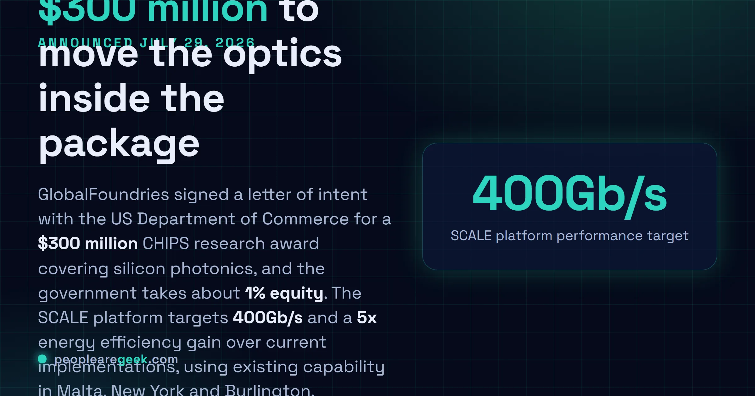
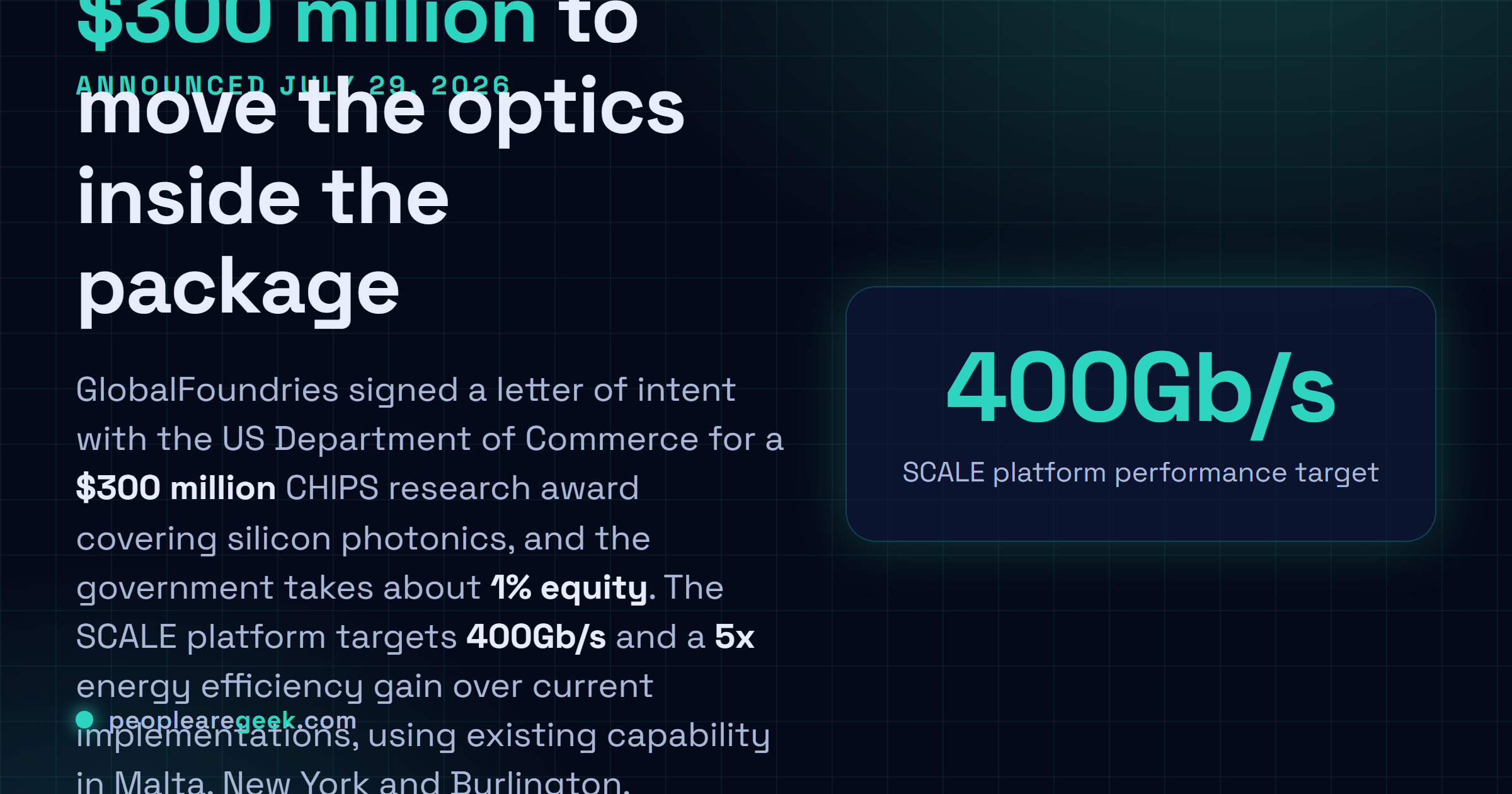
GlobalFoundries signed a letter of intent with the US Department of Commerce on July 29, 2026 for a $300 million CHIPS research award aimed at silicon photonics, and a separate agreement gives the government about 1% of the company. The money funds optical materials, photonics wafer technologies and advanced packaging with 3D hybrid bonding, all pointed at near packaged and co packaged optics. The target platform is called SCALE, and GlobalFoundries quotes 400Gb/s performance with a fivefold energy efficiency gain over current implementations. For network engineers the interesting part is where the optics ends up: on the substrate, next to the switch ASIC, instead of in a cage on the front panel.
The short answer
GlobalFoundries announced on July 29, 2026 that it signed a letter of intent with the US Department of Commerce for a $300 million CHIPS research and development award covering silicon photonics. The work funds next generation optical materials, photonics wafer technologies and advanced packaging including 3D hybrid bonding, enabling near packaged optics and co packaged optics. The target platform, SCALE, aims at 400Gb/s and a 5x energy efficiency improvement over current generation implementations, using existing capability in Malta, New York and Burlington, Vermont. A separate agreement gives the Department of Commerce about 1% of the company.
Most CHIPS announcements are about fabs, and this one is not. There is no new building in it. What GlobalFoundries got funding for is the unglamorous middle of the stack, the part that decides how a bit gets from a switch ASIC onto a fibre without spending most of its energy budget crossing a circuit board first.
What the award covers
The letter of intent is with the CHIPS research and development office at the Department of Commerce, for $300 million. It funds three things: next generation silicon photonics wafer technologies, novel optical materials, and advanced packaging including 3D hybrid bonding. The purpose of all three is to enable near packaged optics and co packaged optics for AI and high performance computing systems.
The platform being advanced is called SCALE, short for Silicon Photonics Co Packaged Advanced Light Engine. GlobalFoundries states the targets as modularity, 400Gb/s performance and a 5x increase in energy efficiency over current generation implementations. The work runs through existing capability at Malta, New York and Burlington, Vermont.
A separate agreement attached to the award gives the Department of Commerce an equity stake of about 1% in GlobalFoundries. That structure has become the norm for these awards rather than the exception, and it is worth registering as a policy fact rather than a technical one.
Where the optics sits, and why it is moving

The reason any of this is happening is that electrical signalling does not scale gracefully with bandwidth. Push more bits per second down a copper trace and you spend disproportionately more power on the serialiser, the equaliser and often a retimer, plus you fight loss and crosstalk over a longer distance.
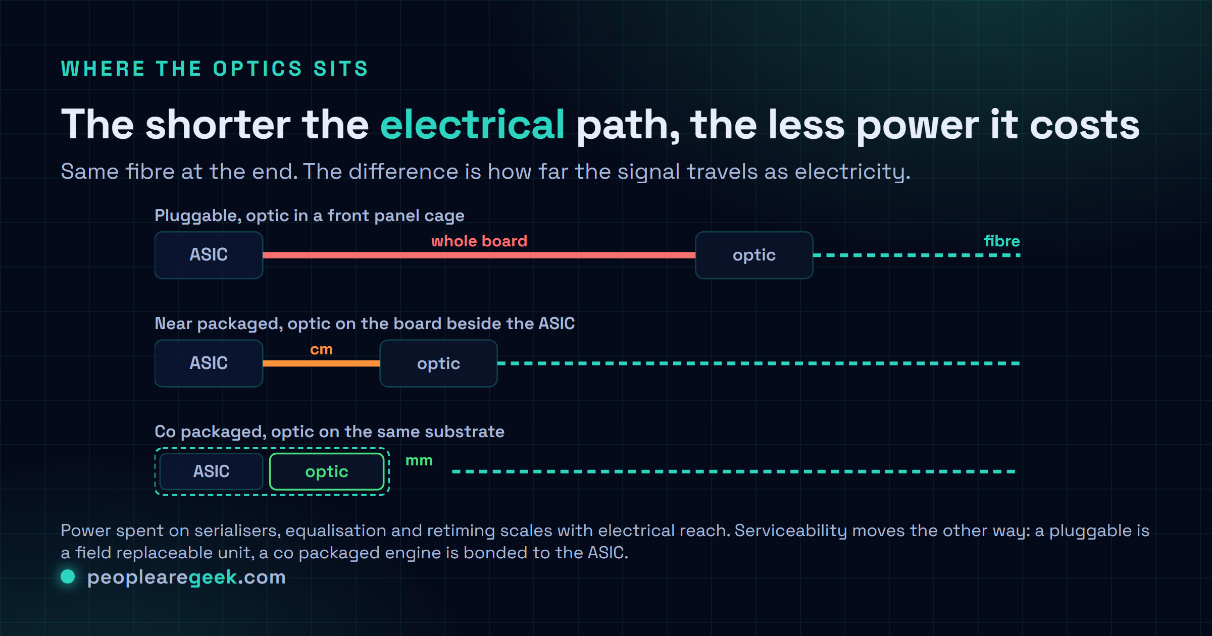
Three placements, in order of how far the signal travels as electricity:
A pluggable transceiver sits in a cage on the front panel. The electrical signal crosses the entire board from the switch ASIC to the faceplate. This is what almost everything in production uses today, and its great virtue is that a technician can swap one in under a minute.
Near packaged optics, or NPO, moves the optical engine onto the same board within a few centimetres of the ASIC. Most of the board traversal disappears.
Co packaged optics, or CPO, puts the optical engine on the same substrate as the switch ASIC. The electrical path is now millimetres, and the power spent driving it falls accordingly.
At the port densities an AI fabric needs, transceivers can consume a large fraction of a switch's total power. That is the budget these platforms are attacking, and it is the same pressure behind NVIDIA's 102.4 Tbps Spectrum-6 generation.
The operational trade nobody puts in the press release
CPO buys power and density, and it charges for it in serviceability.
A pluggable optic is a field replaceable unit. When it fails, the failure domain is one small part with a well understood replacement procedure and a spares cupboard. When a co packaged optical engine fails, it is bonded into the same package as a switch ASIC that cost considerably more than the optic, and the failure domain is that whole assembly.
This is the question we would put to any vendor pitching a co packaged optics switch, in this order. What is the measured failure rate per optical lane, and over what population? Are the lasers integrated or externally supplied, since an external laser module is separately replaceable and integrated lasers are not? What is the field procedure when one lane of many dies, and does it take the whole switch out of service? And what does the spares model look like, given that the spare is now a switch rather than a transceiver?
None of that argues against the technology. It argues for asking about it before the first deployment rather than after the first failure.
The endorsement list is the real signal
The announcement carried supporting quotes from AMD, Broadcom, Cisco, Corning, Lumentum, Marvell, Meta, Microsoft, NVIDIA and Qualcomm. Research awards do not usually arrive with ten named companies attached.
Look at what that list covers. Chip designers who need the interconnect to hit their own roadmap numbers. Optical component vendors. Corning, which makes the glass and fibre. And two hyperscalers who operate the fabrics this is meant to feed, one of which is currently telling investors that cloud demand exceeds the capacity it can bring online. The demand side of this technology is not a projection.
GlobalFoundries shares rose about 9.5% in premarket trading. On a market capitalisation of its size, $300 million of research funding does not explain that move. The customer list does.
What to take from it
Nothing in this announcement changes what you can buy this quarter. It is research money with a target attached, and 400Gb/s with a 5x efficiency gain is a goal rather than a measurement.
What it does confirm is the direction. The industry has decided that optics belongs inside the package, that the domestic supply chain for it is a policy priority, and that essentially every company that would consume the output agrees. If you are writing a data center refresh plan that reaches into 2028 or beyond, co packaged optics is now a thing to design questions around rather than a thing to watch.
Sources and further reading
- GlobalFoundries press release on the $300 million letter of intent
- Full release with supporting quotes on GlobeNewswire
- HPCwire: GlobalFoundries to receive $300M CHIPS award for silicon photonics R&D
- Fibre Systems: GlobalFoundries awarded $300m for silicon photonics R&D
- Quartz: GlobalFoundries wins $300 million CHIPS Act silicon photonics award
Frequently asked questions
What exactly did GlobalFoundries sign, and is the money guaranteed?
It is a letter of intent with the CHIPS research and development office at the US Department of Commerce for a $300 million award, announced on July 29, 2026. A letter of intent is a step before a definitive agreement, so the funds are committed in principle rather than disbursed. A separate agreement tied to the award gives the Department of Commerce an equity stake of roughly 1% in GlobalFoundries, which follows the pattern the current administration has applied to other semiconductor awards. The company said the work leverages existing capability at its Malta, New York and Burlington, Vermont sites rather than a new greenfield fab, so this is research and development money rather than construction money.
What is SCALE, and what do the 400Gb/s and 5x figures refer to?
SCALE stands for Silicon Photonics Co Packaged Advanced Light Engine, and it is the platform the award is meant to advance. GlobalFoundries describes the targets as industry leading modularity, 400Gb/s performance and a 5x increase in energy efficiency over current generation implementations. Read that comparison carefully, because it is against existing silicon photonics implementations rather than against copper cabling in general. Some coverage restated it as a fivefold gain over copper, which is a different and stronger claim than the one in the press release. As with any roadmap number attached to a research award, it is a target rather than a measured product result.
What is the difference between pluggable, near packaged and co packaged optics?
It is a question of how far the electrical signal has to travel before it becomes light. With pluggable optics, the transceiver sits in a cage on the front panel of the switch, and the electrical signal crosses the whole board to get there. Near packaged optics, or NPO, moves the optical engine onto the same board very close to the switch ASIC, cutting that electrical reach to a few centimetres. Co packaged optics, or CPO, puts the optical engine on the same substrate as the ASIC, so the electrical path is millimetres. Shorter electrical reach means less power spent on serialisers, equalisation and retiming, which is where most of the energy saving in these platforms comes from.
Why does co packaged optics matter for people who run networks rather than design them?
Two operational consequences, and they pull in opposite directions. The good one is power and density: at the port counts a modern AI fabric needs, the transceivers can account for a large share of a switch's power budget, and moving the optics onto the substrate cuts that. The awkward one is serviceability. A failed pluggable is a field replaceable unit that a technician swaps in a minute. A failed co packaged optical engine is attached to the switch ASIC, so the failure domain becomes the whole package. Anyone evaluating this generation of hardware should be asking vendors about optical link failure rates, external laser sourcing and what exactly gets replaced when a lane dies.
Who else is backing this, and why does that list matter?
The announcement carried supporting statements from AMD, Broadcom, Cisco, Corning, Lumentum, Marvell, Meta, Microsoft, NVIDIA and Qualcomm, which is close to the complete set of companies that would buy or integrate the output. That is unusual for a research award and tells you the demand side is not speculative. It also spans the whole stack: chip designers who need the interconnect, optical component makers, a glass and fibre supplier, and two hyperscalers that operate the fabrics. GlobalFoundries shares rose roughly 9.5% in premarket trading on the news, which is the market pricing the customer list rather than the $300 million.