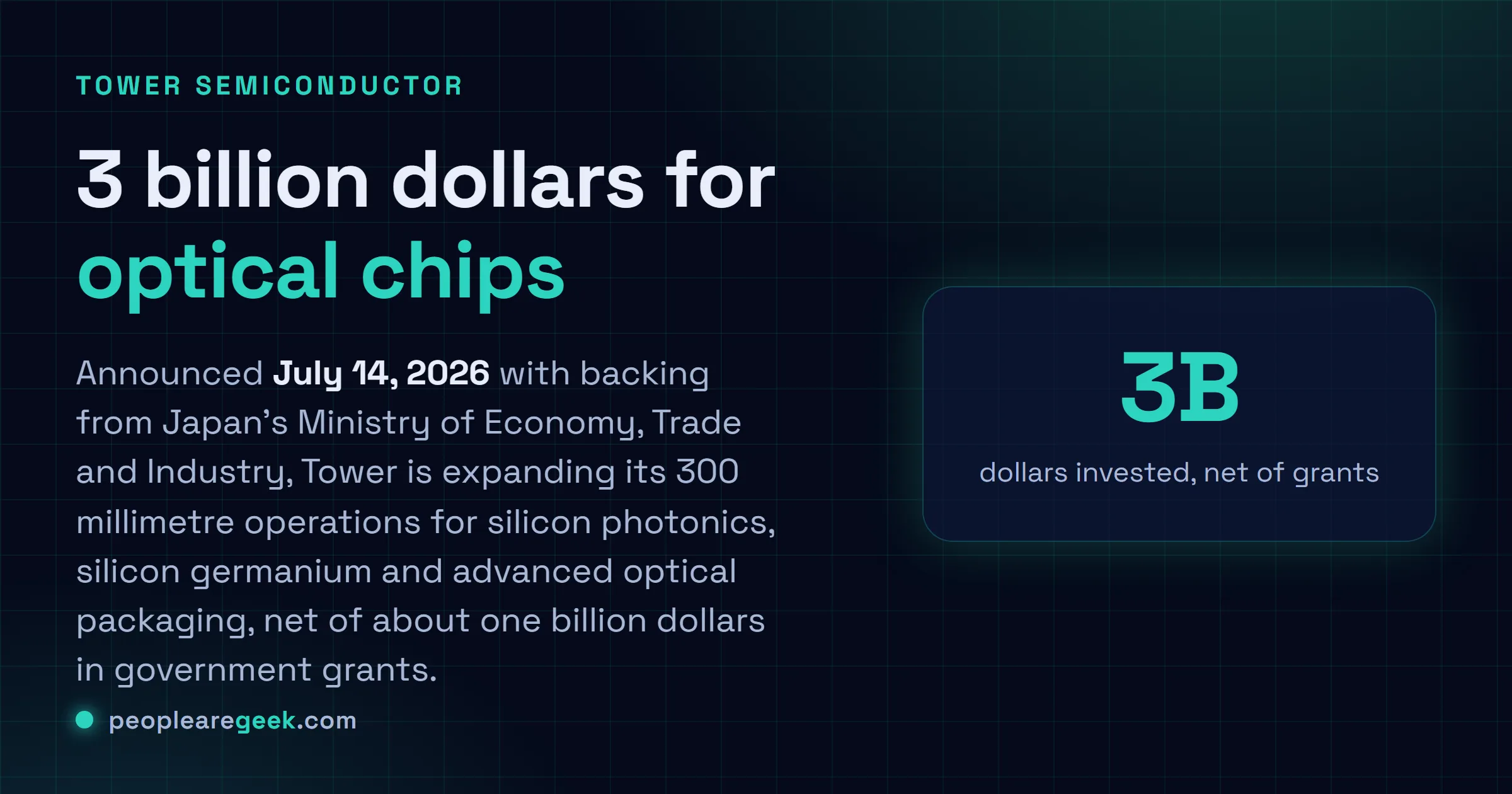
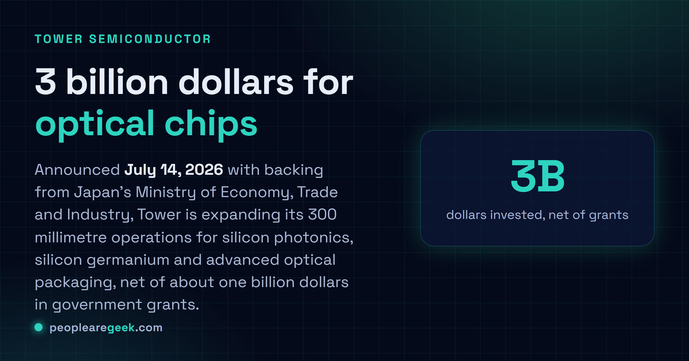
Tower Semiconductor is spending about three billion dollars to expand its 300 millimetre operations in Japan, with roughly one billion dollars of grants from the Japanese government behind it. Announced on July 14, 2026 with backing from Japan's Ministry of Economy, Trade and Industry, the plan covers silicon photonics, silicon germanium, and advanced optical packaging. These are the parts that move data between AI accelerators rather than doing the maths inside them. It is a useful reminder that the bottleneck in a modern AI cluster is often not the compute at all. It is the interconnect, and the interconnect is going optical.
The short answer
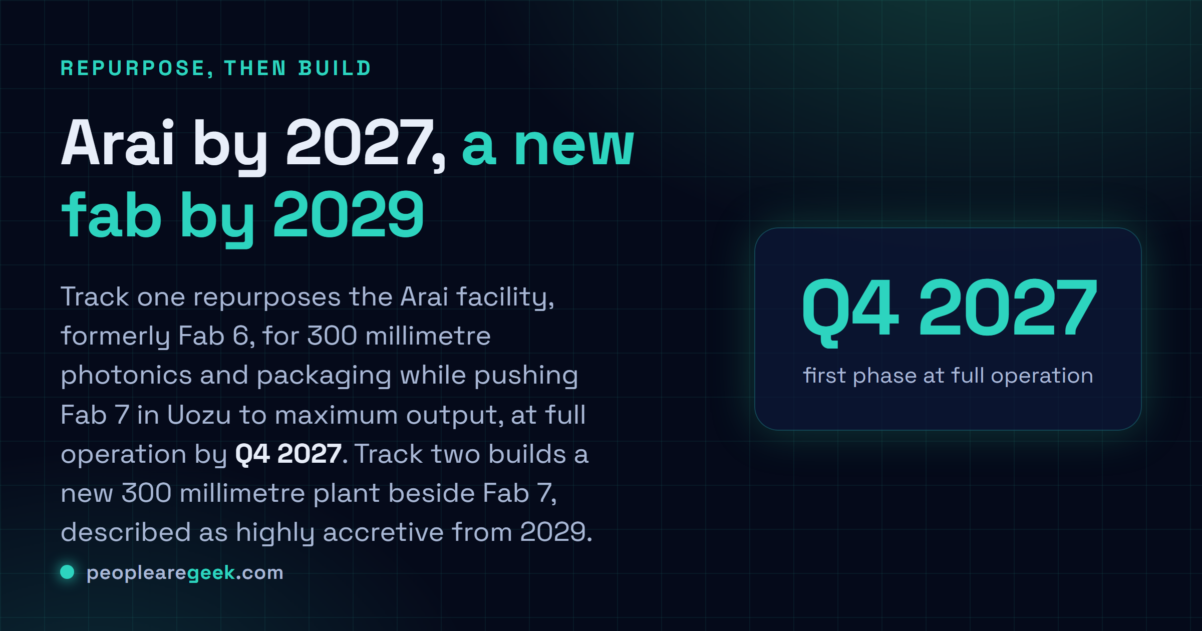
Tower Semiconductor is investing about three billion dollars to expand its 300 millimetre operations in Japan, net of roughly one billion dollars in grants from the Japanese government, announced July 14, 2026 with backing from the Ministry of Economy, Trade and Industry. The programme covers silicon photonics, silicon germanium, and advanced optical packaging for AI data centre interconnect. It runs on two tracks, repurposing the Arai facility for 300 millimetre photonics with full operation by the fourth quarter of 2027, and building a new plant beside Fab 7 in Uozu that Tower expects to be highly accretive from 2029.
Most coverage of the AI build out counts accelerators. How many GPUs, on what node, in whose data centre. That is a reasonable way to count, but it quietly assumes the interesting scarcity is arithmetic. Spend time near an actual training cluster and you learn the real fight is often about moving data, not crunching it. Tower Semiconductor just put three billion dollars behind that second problem.
What was announced
On July 14, 2026, Tower Semiconductor said it will spend roughly three billion dollars expanding its 300 millimetre operations in Japan, net of about one billion dollars in grants from the Japanese government. The announcement came with backing from Japan's Ministry of Economy, Trade and Industry, which is the part that tells you Tokyo considers this strategic rather than merely commercial.
The programme covers three related things. Silicon photonics, the optical components that turn data into light and back. Silicon germanium, the process used for the very high speed analogue circuits that drive those optical parts. And advanced optical packaging, the assembly work that puts the pieces together. All of it points at one market, the optical interconnect inside AI data centres.
The build runs on two tracks. The first repurposes the Arai facility, formerly Fab 6, for 300 millimetre silicon photonics and packaging, while pushing Fab 7 in Uozu to its maximum output. Tower expects full operations there by the fourth quarter of 2027. The second track builds an entirely new 300 millimetre plant next to Fab 7, which the company says should deliver a multi fold increase in silicon photonics and silicon germanium capacity, and be highly accretive from 2029.
Why the interconnect became the bottleneck
Here is the part worth understanding if you work anywhere near networks.
Training a large model is not one big calculation. It is an enormous number of medium sized calculations spread across many accelerators that must constantly exchange results with each other. Every time the cluster synchronises, data crosses the links between chips. If those links are slower than the chips, the chips wait. You end up with a room full of extremely expensive silicon idling because the network underneath it could not keep up.
Copper has been the default for short links, and copper is genuinely good at short distances. Its problem is that as signalling rates climb, the distance you can drive a copper link before the signal degrades keeps shrinking. Push hard enough and copper works within a rack and struggles between racks. That is exactly the range where AI clusters need bandwidth, which is why the industry keeps moving the optical boundary closer to the chip.
Optics solves the distance problem and carries more bandwidth per watt, but historically optical parts were made in specialist processes at specialist volumes and priced accordingly. Silicon photonics is the answer to that. Build the optical parts on standard silicon lines, in a 300 millimetre fab, using the manufacturing machinery the industry already knows how to run at scale. That is what makes optics affordable at data centre quantities, and it is precisely the capacity Tower is adding.

What the money signals
Tower raised its own outlook alongside the news, which is the clearest statement of how it reads demand. The company now expects about 3.6 billion dollars of revenue and about 1.2 billion dollars of net profit in 2028, up from previous expectations of 2.8 billion dollars and 750 million dollars. That is a substantial revision, and it is a revision made on the strength of parts that carry data rather than parts that process it.
The government grant is the other signal. Roughly one billion dollars of public money, with METI backing, says Japan wants domestic capacity in optical components specifically. Advanced manufacturing has become concentrated in ways that make a lot of governments uncomfortable, and optical interconnect is a chokepoint with real leverage. If you cannot get the parts that connect accelerators, owning the accelerators does not help much.
The takeaway
The useful frame is this. Compute capacity and network capacity are not separate budgets in an AI cluster, they are one constraint measured at two points, and the binding one has been drifting toward the network for a while. A three billion dollar investment in optical components, with a government paying for a third of it, is what that drift looks like when it reaches the balance sheet.
For anyone whose job touches data centre networking, the practical read is that the optical boundary keeps moving closer to the silicon, and the supply of parts to make that possible is being expanded on a 2027 to 2029 timeline. That is the horizon on which the economics of high speed interconnect are likely to change, and it is worth knowing before the specs land rather than after.
Sources and further reading
- Reuters via Yahoo Finance: Tower Semiconductor to invest 3 billion dollars in Japan, backed by government grants
- CTech: Tower Semiconductor to invest 3 billion dollars in Japan expansion as AI drives demand for optical chips
- TipRanks: Tower Semiconductor launches 3 billion dollar Japan expansion in silicon photonics and SiGe
- The Next Web: Tower Semiconductor puts 3bn into Japan, and Tokyo is paying for a third of it
- Proactive Investors: Tower Semiconductor shares jump on Japan expansion to boost silicon photonics capacity
Frequently asked questions
What did Tower Semiconductor announce?
On July 14, 2026, Tower Semiconductor announced a roughly three billion dollar expansion of its 300 millimetre operations in Japan, net of about one billion dollars in grants from the Japanese government, with backing from the Ministry of Economy, Trade and Industry. The programme covers silicon photonics, silicon germanium, and advanced optical packaging, all aimed at optical components for AI data centres.
What is silicon photonics in plain terms?
Silicon photonics means building optical components, the parts that send and receive light, using the same silicon manufacturing processes used for ordinary chips. Instead of moving data as electrical signals down copper, you move it as light down fibre or waveguides. The appeal is that light carries more bandwidth over longer distances for less power, and making it in a standard silicon fab is what brings the cost down to data centre volumes.
Why does an optical chip investment matter for networking?
Because the interconnect is increasingly what limits a large AI cluster, not the accelerators. Training a large model means constantly shuffling data between many GPUs, and if the links between them cannot keep up, expensive silicon sits idle waiting. Optical interconnect is the current answer to that limit, so capacity for optical components is effectively capacity for cluster scale.
What are the two parts of the expansion?
The first repurposes the Arai facility, formerly Fab 6, for 300 millimetre silicon photonics and packaging while pushing Fab 7 in Uozu to maximum output. Full operations there are expected by the fourth quarter of 2027. The second builds an entirely new 300 millimetre plant next to Fab 7, which Tower expects to deliver a multi fold increase in silicon photonics and silicon germanium capacity and to be highly accretive from 2029.
What is silicon germanium used for here?
Silicon germanium is a process technology suited to very high speed analogue and mixed signal circuits. In an optical link, something has to drive the laser and amplify the faint signal arriving at the far end, at the speeds modern transceivers run. SiGe is a common choice for those driver and amplifier roles, which is why it sits alongside silicon photonics in the same investment rather than being a separate business.
What does Tower expect to earn from this?
Tower raised its outlook alongside the announcement. It now expects 2028 revenue of about 3.6 billion dollars and net profit of about 1.2 billion dollars, compared with previous expectations of 2.8 billion dollars of revenue and 750 million dollars of net profit. The new plant next to Fab 7 is described as highly accretive from 2029, so the larger effect lands after the 2028 figures.